IBM unveils 0.7nm nanostack chip technology as a research milestone
The approach builds transistors upward in three dimensions. The node name is not a literal measurement of every feature on the chip.

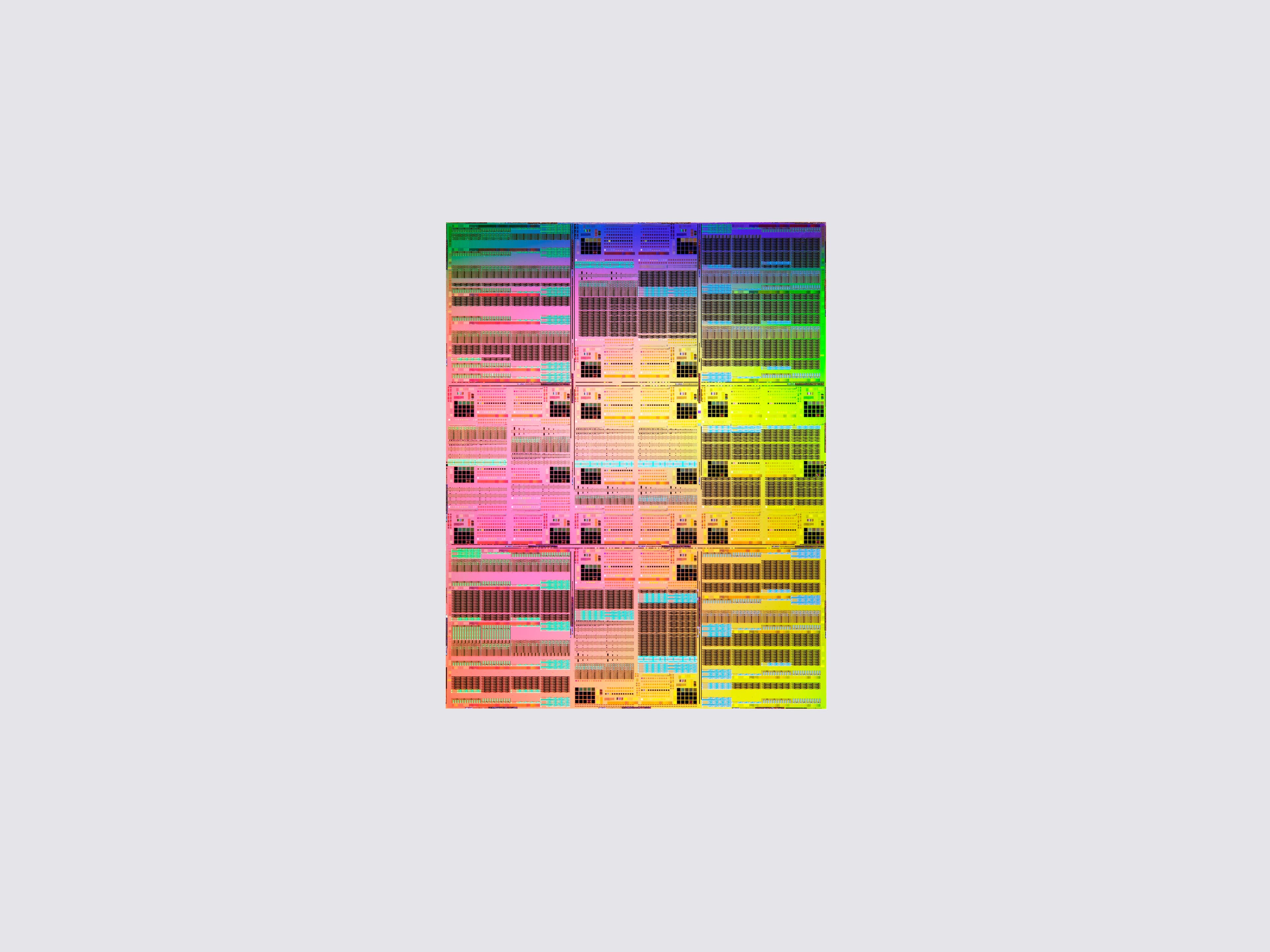
Building upward
IBM announced sub-1nm chip technology on June 25, 2026, describing a 0.7nm, or 7-angstrom, node based on its nanostack architecture.
The company reported roughly 100 billion transistors on a small chip and projected gains compared with IBM's 2nm technology. These are company research claims, not our measurements of a consumer product.
What does nanostack change?
IBM Research describes moving transistor arrangement into three dimensions. Instead of limiting expansion to a flat surface, the design places components above others.
One element is the sequential stacking of n-type and p-type transistors, allowing materials to be optimized for each. Connecting the layers introduces its own challenges in alignment, manufacturing and fine wiring.
IBM's research explanation also covers wafer-bonding advances and denser SRAM. This matters because useful computing depends on more than arithmetic units alone: memory and interconnects must function with them as part of a complete design.
What does 0.7nm mean?
IBM's announcement explains that process-node names describe generations of manufacturing technology, not a single literal dimension shared by every component. It would therefore be wrong to infer that every wire or transistor feature is 0.7 nanometers wide.
The significance lies in architecture, density and the potential for further development. Focusing only on a smaller number can give readers a misleading picture of what was demonstrated.
When could it reach devices?
This is a research announcement. IBM sees a potential path to production in as early as five years. That is a projection rather than a guaranteed retail date for a particular phone or computer.
Our interpretation is that important questions remain between laboratory work and a product: what will manufacturing cost, how many usable chips can be made, how will heat be managed, and will suitable design tools be available?
A research breakthrough can open an important direction for the industry, but it does not replace answering those questions. Demonstrating a concept and supplying a commercial processor at scale are different achievements.
Keeping that distinction clear makes it possible to appreciate the work without turning it into an immediate promise about battery life or speed in devices that have not been announced.
Sources
Founder and editor-in-chief of Kurd Developers. Phone and tech news on YouTube, Instagram and TikTok.
More stories

One text can break your phone: Android's 'SMS of Death' explained
A flaw in Android 12 and later lets a specially crafted SMS drop calls and even make a phone unusable. The fix is in October's security patch.

GTA VI lands November 19: prices, editions and what to know
Rockstar has locked the date: Thursday, November 19 on PS5 and Xbox Series X|S. Standard costs $79.99 and Ultimate $99.99.

Apple's first touchscreen MacBook Pro brings OLED and Dynamic Island
The new PROLED XDR display responds to touch, the notch is gone and Dynamic Island takes its place. Prices start at $2,899.

The $1,999 iPhone Duo Has a Black-Bar Problem, and Fixing It Is Harder Than It Looks
Apple's first foldable is a hardware flex. But unfold it and many of your apps shrink into a phone-shaped window floating in black. Here's why the app world wasn't ready, and why developers can't just hit "stretch".